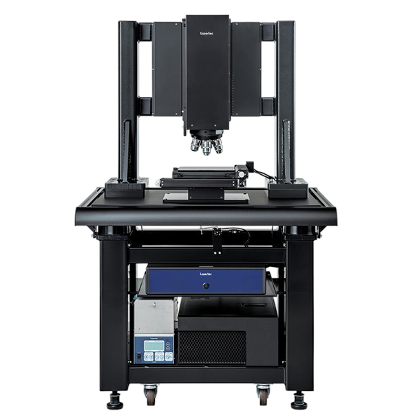
OPTELICS IR
OPTELICS IR is an effective tool for observing the internal structure of silicon wafers and devices made from IR-transmissive materials. In the rapidly growing advanced packaging market, it is especially suited for R&D and process optimization applications such as alignment measurement, void detection, and adhesive peeling observation.
Features
High-brightness IR confocal optics
High-resolution observation at wavelengths from 1000nm to 1500nm
High-accuracy measurement in the XY directions
Height measurement using optical sectioning in the Z-axis direction
Applications
Observation of the internal structure of IR-transmissive materials such as silicon wafers
Inspection and evaluation of 3D packaging
Analysis of internal defects in advanced packaging devices
Non-destructive etching volume measurement in oxide sacrificial layer etching
Lamination alignment measurement
SOI active layer thickness measurement