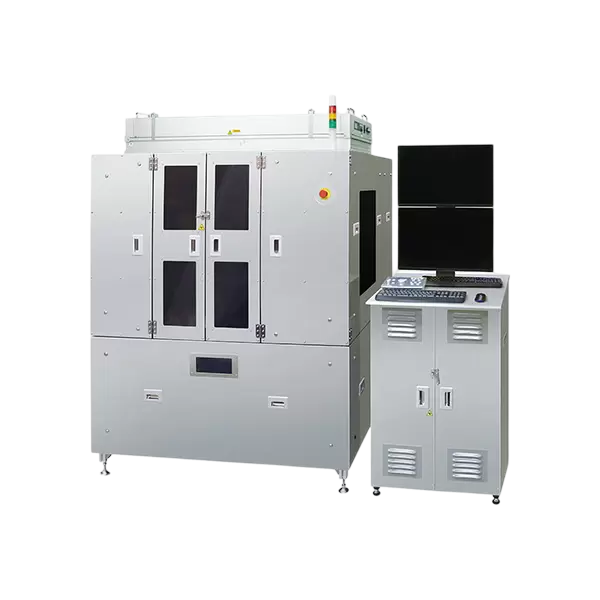
OPTELICS AI²
OPTELICS AI² performs automatic defect inspection, high-magnification defect review, and 3D surface shape profiling in one device. It supports both R&D and production workflows that require speed, precision, and flexible defect analysis.
Features
Automatic defect inspection, high-magnification review, and surface shape profiling of various types of semiconductor wafers in a single device
High-speed inspection capability: a whole 3-inch wafer in 15 minutes with sub-micron sensitivity
High-magnification review capability with objective lens switching
Deep learning-based high-precision image classification, patterned sample inspection, and specific defect-type inspection
Defect inspection, review, and surface shape profiling of transparent samples such as compound semiconductors and films without backside reflection interference
Complete hardware and software system support with customization for specific customer needs
Applications
High-speed automatic defect inspection of various types of semiconductor wafers
Defect review
Defect surface shape profiling
Defect tracking in production process
Specifications
| Inspection time (3" wafer) | 15 minutes per wafer |
|---|---|
| Samples | Various types of semiconductor wafers (including silicon, SiC, GaN, InP, AlN and glass), glass substrates, films, and others |
| High-speed automatic surface defect inspection | Confocal and differential interference contrast optics |
| High-magnification defect review | Confocal optics |
| Defect shape 3D profiling | Available |