
CIEL Series
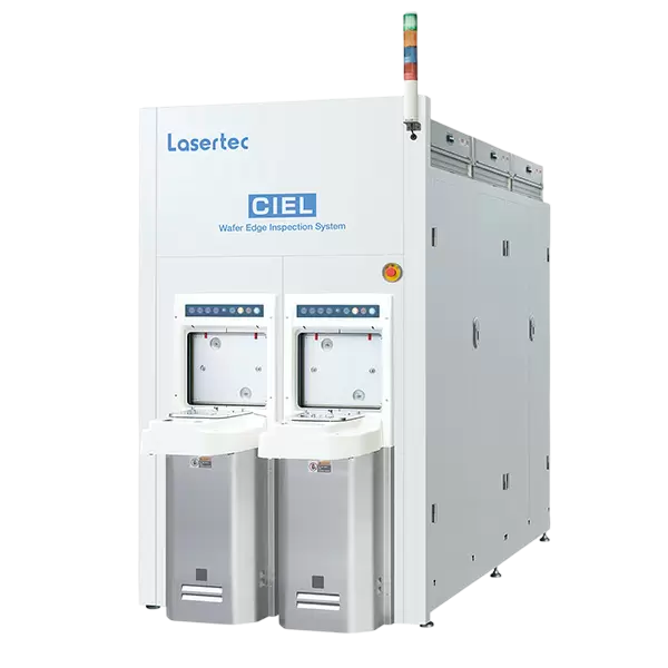
Features
Detection of micro defects that could not be detected or classified with conventional methods
High-precision defect classification using deep learning technology
High-sensitivity, high-throughput inspection with proprietary optical system
3D measurement for process improvement
Applications
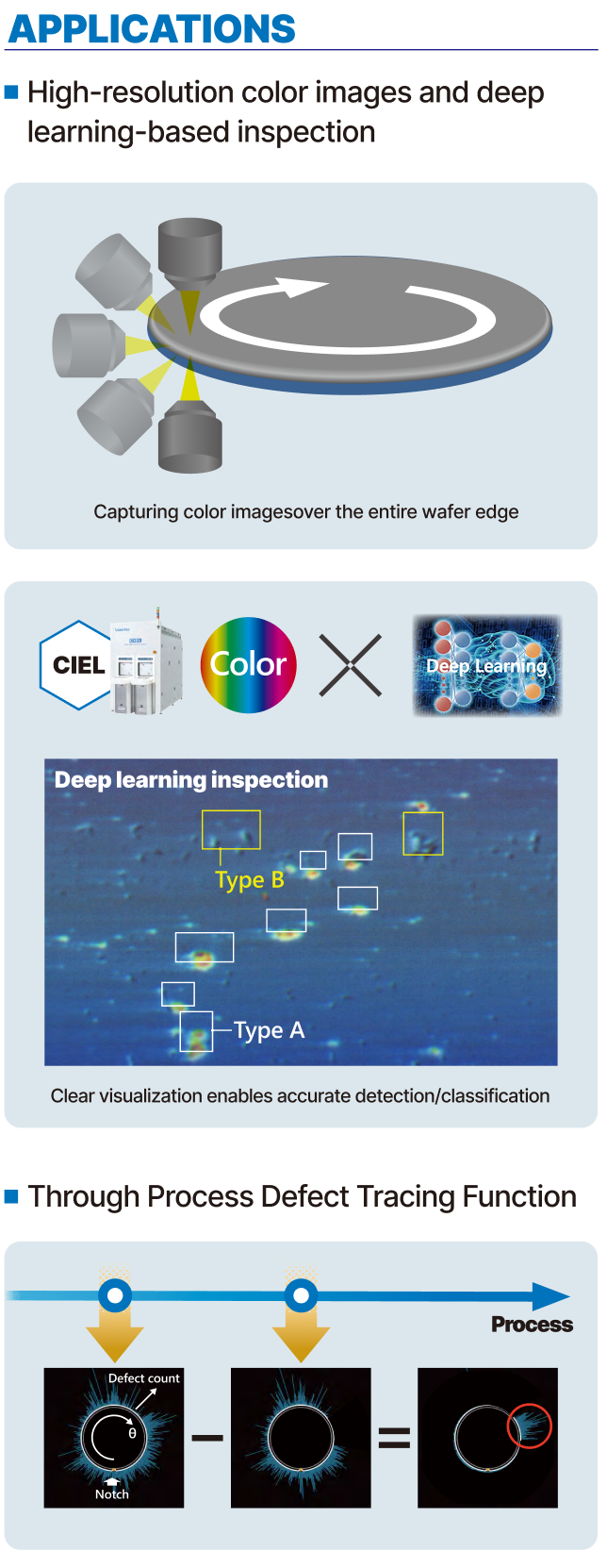
Detection of micro defects that could not be detected with conventional methods
High-precision defect classification using deep learning technology
Extraction of defects directly related to yield
3D measurement for process improvement
Specifications
| Dimensions (mm) | 1,450mm(W) x 2,650mm(D) x 1,885mm(H) |
| Applicable wafer size | 300 mm wafer |
| Detection capability | Micro defects with high sensitivity |
With the miniaturization and high layering of semiconductor devices, defect types originating from wafer edges are increasing and detection sizes are becoming smaller. There is a demand for equipment that can detect and classify only the defects that reduce yield from among these diverse defects.
CIEL has completely renewed the optical system of the EZ Series and achieved high-sensitivity, high-throughput inspection with a proprietary optical system. In addition, high-precision defect classification using deep learning technology and the 3D function of the proprietary optical system enable acquisition of high-resolution images including height and depth information, and have enhanced the function to identify defects that should be detected.